Saturday, January 22, 2011

Practical guidelines for PCB design

This is a very basic list of points important in the design of printed circuit boards (PCB). It is based in a lecture given by Jhonny Chee from the Polytechnic Ngee Ann from Singapore in the Chiba University in October 2010

There are two main problems to deal with when we are working on the design of PCB´s. 

  1. Reduce the noise that might affect the circuit behavior itself
  2. Avoid to produce electric that contaminate the power supply network or the surrounding devices.

in the successive we will name some common sources of the above mentioned problems and the way to minimize their undesired effects.

Stray capacitances: It exists between any two conductors. If the stray capacitance is large enough, aimage small current can “jump” trough the capacitance and contaminate the signal traveling in the near conductors. This is specially annoying when we have high frequency components in our circuit.

Techniques to minimize this capacitance:

  • Widening the separation between conductors
  • Shortening the conductors lines.
  • Guarding (Putting ground lines “covering” the signal lines)

Radiated emission: Electromagnetic noise originated by the conductors in our circuit that could act as a antenna.

Techniques to minimize this problem:

  • Try to reduce the area covered by the conductors carrying high frequency signals, for example, always try to put the supply and return conductors running parallel.
  • Shield the electromagnetic sensible circuits (covered with a metallic cap connected to ground, or surround it by a ground plane)
  • Use ferrite choke. Ferrite increase the magnetic permeability increasing  the inductance imagewhich  is “see” as impedance by the high frequency currents. Using ferrite choke at the input or output of the power supply will “clean” the signal of high frequency components. This is very effective for common mode interference but do not affect differential signals.

General tips.

- Always try to use a ground plane (a side of the PCB as ground)

- Create your own library including all the components you will use. This tip reduce time when designing the PCB and minimize errors selecting wrong devices not in stock.

- Use always decoupling capacitors ( minimize the noise in the power supply for each device,usually 0.1uF, 0.01uF) and try to attach it as close as possible to the device using them. Decoupling capacitors are not effective far from the “protected device”.

-  Try to allocate pin 1 of each connector as ground. This practice makes easier to locate the ground point in each connector.

- Use a spreadsheet to aid in the pin assignment listing functions of each pin.

- Include tests points  and one or more ground pads. It makes easier to debug your circuit. Only use tests points for stages of the circuit or for the most important signals, do not over use the test points. Place the ground pads close to the edge of the PCB, is easier to identify and to connect using crocodile clips.

- Always try to use connectors to connect your circuit with the real world. Is easier to test and debug than is you connect your circuit using soldered wires.

- Group components together according to their intended function giving priority to the shorter path rather than aesthetics.

- Prioritize component placement in the next order:

  1. Decoupling (closest to the IC keeping copper paths short)
  2. High frequency (place components to minimize track length. This reduces radiated interference)
  3. High sensitivity (Put inputs of signals close to their amplifiers to avoid pick up noise and amplifier it)

- Routing order priority:

  1. Within functional group (first route between components of a functional stage and the interconnections with other stages )
  2. inter-group

- Minimize length of tracks in the ground plane. This preserves the properties of the ground plane.

- Use via holes to connect ground components to the ground plane. (shorter routes to ground allowing space on the routing plane for interconnect components signals)

-  Use thicker tracks for power lines. (power lines carry more current and need more cooper to do that efficiently)

- Avoid use breaks in the power lines. Using many breaks  will increase the track impedance.

- place text strings to identify components.

- Check and optimize your layout.

  • Verify footprints match with the real component in stock.
  • Verify connections looking weird.
  • Verify that the decoupling capacitors are near to the IC´s-
  • Incoming power has a large capacitor?
  • Adjust clearance between tracks and vias.
  • Check the ground plane (usually the bottom side), it is not braked by signal tracks?
  • Remove any island of floating copper (This increase the crosstalk). If it can not be removed connect it to ground.
  • Attach connecting vias around the edge to ground in order to block the EMI (electromagnetic interference)

Happy PCB design, soldering and use! Sonrisa
Tuesday, November 2, 2010

Finding the area of an amorphous figure in MATLAB

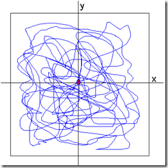
Imagine that you have two series of data (nx1). Imagine that these data come from two sensors measuring the displacement of a particle around a certain point, something like this:image
  The sensors measure the position X-Y 100 times each second and you measure for 30 seconds. At the end you will have two vectors containing 3000 samples each one.
Something like this:
x=[3,6,7,5,3,2,3,7,8,9,7,5,3,2,12,3,5,7,8……...n]
y=[2,4,5,6,7,3,5,3,2,5,7,43,6,8,4,2,4,6,7,……..n]
From these vectors of data you must to calculate the area  drawn by the (x,y) values, the contour of the image.

Sunday, October 31, 2010

Electric blanket

Have you ever wonder how an electric blanket works?

Well, Personally I have not wonder that because I Thought had an idea about the basis of this common device. But some days ago somebody give me a small electric blanket and suddenly it stops working. And, you known me, if something can be striped down, it will be striped down! Guiño

Here the pics and the things I saw.

Friday, October 1, 2010

Accelerometer LIS3LV02DL controlled by a dsPIC, I2C communication

This post describe the basic data acquisition of an accelerometer LIS3LV02DL over I2C bus using a dsPIC30F3012.
This tri-axial accelerometer has a 12 or 16 bit digital output and can be interfaced using SPI or I2C communication.
The circuit employed is a very simple one, The dsPIC is connected to the accelerometer LIS3LV02 via I2C using the B7 and B6 pines. The dsPIC reads the data and send the results in ascii format to the PC using the bluetooth module KC21.

Thursday, August 12, 2010

The internal oscillator in the pic12f629

Recently I’ve been using the small pic12f629. My interest was to use it as a cheap D/A converter using PWM. Unfortunately, I chose this pic at the store without check the characteristics first, yeah, I know, how stupid of me! :-(
I thought it had a PWM module as well as a ADC converter, but not, no PWM and no ADC, but anyway, for my purposes it could works! Also, the price was good! just 1000 yen for 10 SO chips plus one DILP!  :-)
So, I present a program to read three inputs “quasi-digital” coming from a FSR sensor and then, according to the inputs, the pic will generate a PWM signal with width of pulse depending on the combination of the input signals.

Friday, August 6, 2010

Analog Digital converter of dsPIC30F3012 using internal ADC clock

I have been reading about the ADC for the dspic30F3012 or the family of these dsPICs.
As I explained in the anterior post, the data sheet mentions an internal clock exclusive for the ADC. From this clock depends the conversion time and then the sampling rate, so, it’s very important to know that data. Surprisingly I didn’t find that data neither the datasheet nor the family reference manual. Probably it exists there but very very hidden. 

Thursday, August 5, 2010

PWM using the dsPIC30F3012 with internal oscillator

This time let’s generate a PWM signal using the dsPIC30F3012 running with its internal oscillator in order to have the RC15 pin available for other applications.
The internal oscillator of this device runs at 7.37MHz and is possible to multiply it by 4, or 16 using the PLL.
In this example I’m using the PLL16 which combined with the 7.37MHz internal oscillator gives a total clock frequency of 117.92MHz, or 29.48 MIPS.
I’m using the circuit depicted below.

Monday, May 24, 2010

USING A SD CARD WITH FAT16, PIC18F2550 and Bluetooth

imageI bet some day we have needed to or wanted to save a large amount of data using the common SD cards and some microcontroller.
For example to save samples of temperature every hour, or every minute, to read pictures and show them in a full color display, or maybe to make an mp3 player. Well the possibilities are huge.
This time I wanted to save EMG signals (Electromyography) from my active EMG sensors. For this reason I made a circuit and a program for the PIC18F2550 microcontroller.
Basically I have to meet two requirements.

Friday, March 19, 2010

dsPIC30F3012 rs232 115200 bps

Now the program and circuit to connect a dsPIC 30F3012 via serial to a PC. The serial connection is made using a Bluetooth module fro kc wirefree (R). The KC21.
BLUETOOTH characteristics
Related Posts Plugin for WordPress, Blogger...