As I explained in the anterior post, the data sheet mentions an internal clock exclusive for the ADC. From this clock depends the conversion time and then the sampling rate, so, it’s very important to know that data. Surprisingly I didn’t find that data neither the datasheet nor the family reference manual. Probably it exists there but very very hidden.
Anyway, after search in forums, and tents of webpages I found a document that explain about that clock, and also how to calculate the sampling rate using the primary clock.
Here is the document.
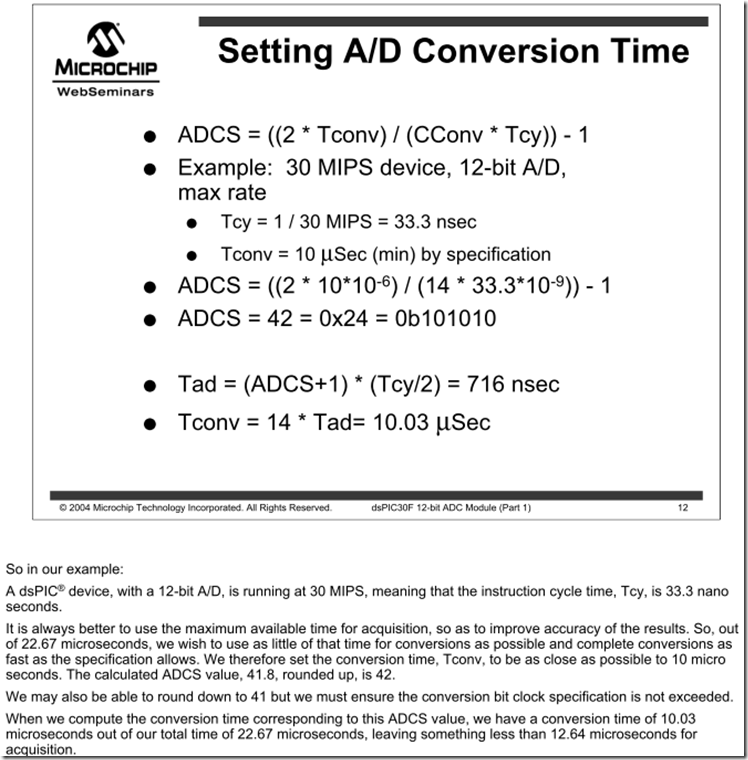
But in case it’s is missed someday, I’ll post here the slide where it’s explained.
As it says, the nominal rate is 47 ksps wich means a conversion time of 21us.
The conversion time is calculated (for a 14 bits ADC) as follows:
Tcon=TAD*14 (multiply by 12 if you are using a 10 bits ADC)
The next figure explain how to calculate the value to write in the ADCS bits of the ADCON3 register in order to get the conversion time desired.
Reading the file you will understand clearly, I hope.
Anyway, I measured the real time of conversion using the internal ADC clock and I got 32us of conversion time.
This is around 12us more than the specified 21us then my maximum sampling rate, without consider the acquisition time, will be around 31 ksps.
Keep this in mid if you are planning to use the dspic to convert data at high speed. For me, now is ok. My sampling rate will be 100Hz. Much more than sufficient! :-)


No comments:
Post a Comment